Repairing a Tektronix PB200 Bert tester – part one

Repairing a Tektronix PB200 Bert tester

The Tektronix PB200 BERT

Before diving into repairing the Tektronix PB200 BERT tester, let me explain briefly what a BERT Tester is. BERT stands for ” bit error rate test ” In the most simple form, a BERT tester sends out a random bit patron, and an analyzer receives the bit pattern and compares this bit pattern to see if there is any bit error.

Obviously this is more complicated, how does the analyzer now what the original bit stream was ? The theory behind it this is quite complex, and beyond the scope of this article. For a more in depth explanation see [this] Wikipedia article.

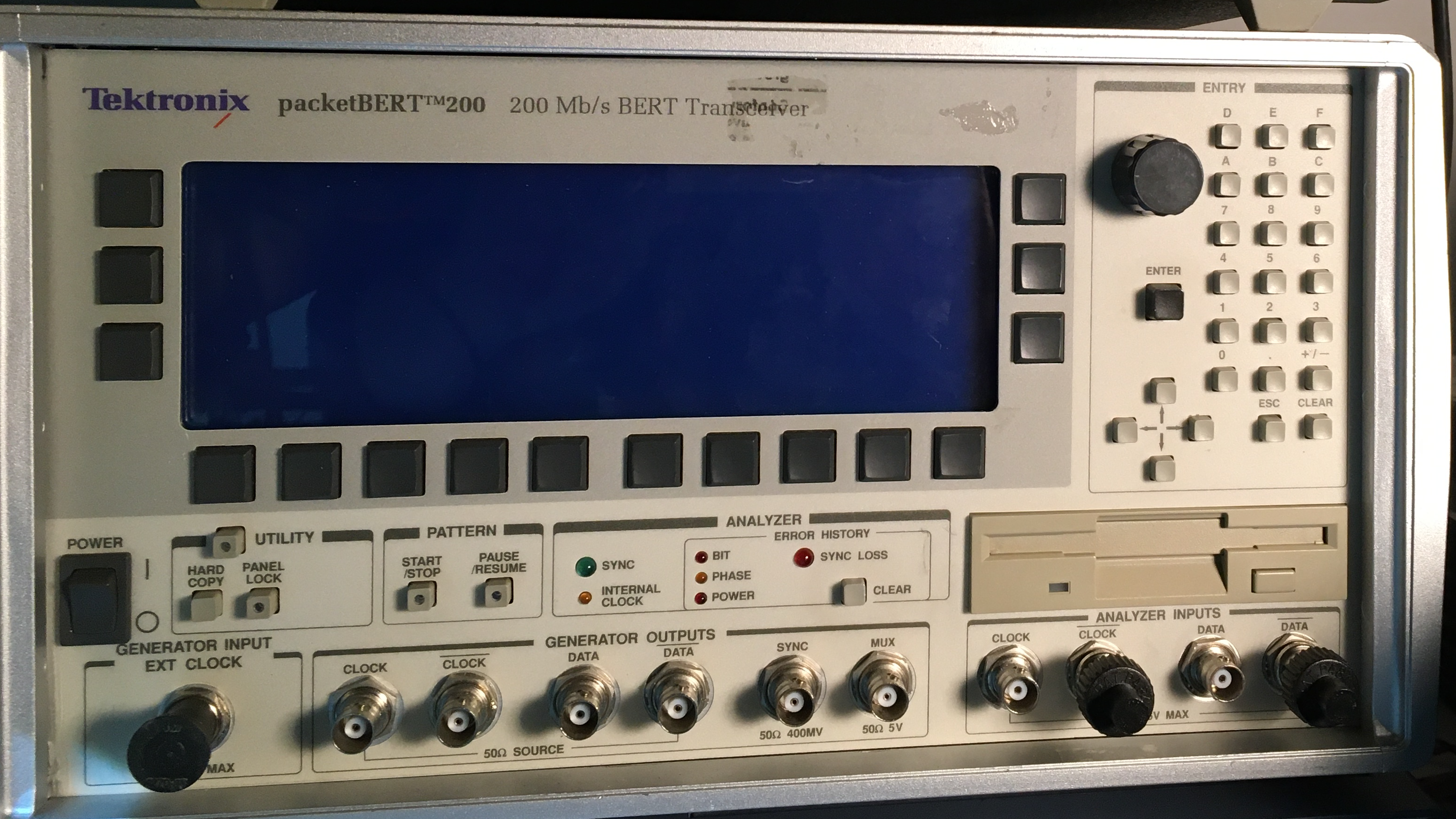
A device like the Tektronix PB200 is used to test different data transmission devices, like optical interfaces, or a like.

The Tektronix PB200 has a data generator and an analyzer built into one device. The specs for this device:

GENERATOR
     Clock Frequency: DC to 200 MHz.
      Amplitude: 0.5 to 5.0 V p-p.
      Termination select: 50 Ohm to -2 V, +3 V, AC or GND.
     Input range: ECL, TTL, PECL compatible.
     Threshold resolution: 10 mV step.
    Internal synthesized clock source: Frequency: 1 Hz to 200 MHz.
    Resolution: 1 Hz.
    Accuracy: 10 ppm.
    BURST clock:
    Programmable gap: 16 Kbits
    maximum, 8-Bit resolution.
Pattern Generator
    PRBS: 2 N- 1, N = 31, 23, 15, 11, 10, 9, 7.
    Programmable word: 256 Kbits maximum, 8-Bit resolution.
    Mark density: PRBS 2 10 1 (1/8, 1/4, 1/2, 3/4, 7/8).
    Mixed mode frame: 256 Kbits maximum, 8-Bit resolution.
    Error injection: Error: Single, Rate, External (TTL).
    Field select: Overhead, payload or both.
    Error rates: Error rate of 10-n, n = 3, 4, 5, 6, 7.
    Outputs: Data and clock outputs:
    Format: NRZ.
    Configurations: Differential (True/Complement).
    Source impedance: 50 Ohm.
    Amplitude: 0.5 V to 2.0 V, 10 mV step.

A Tektronix PB200 which is dead

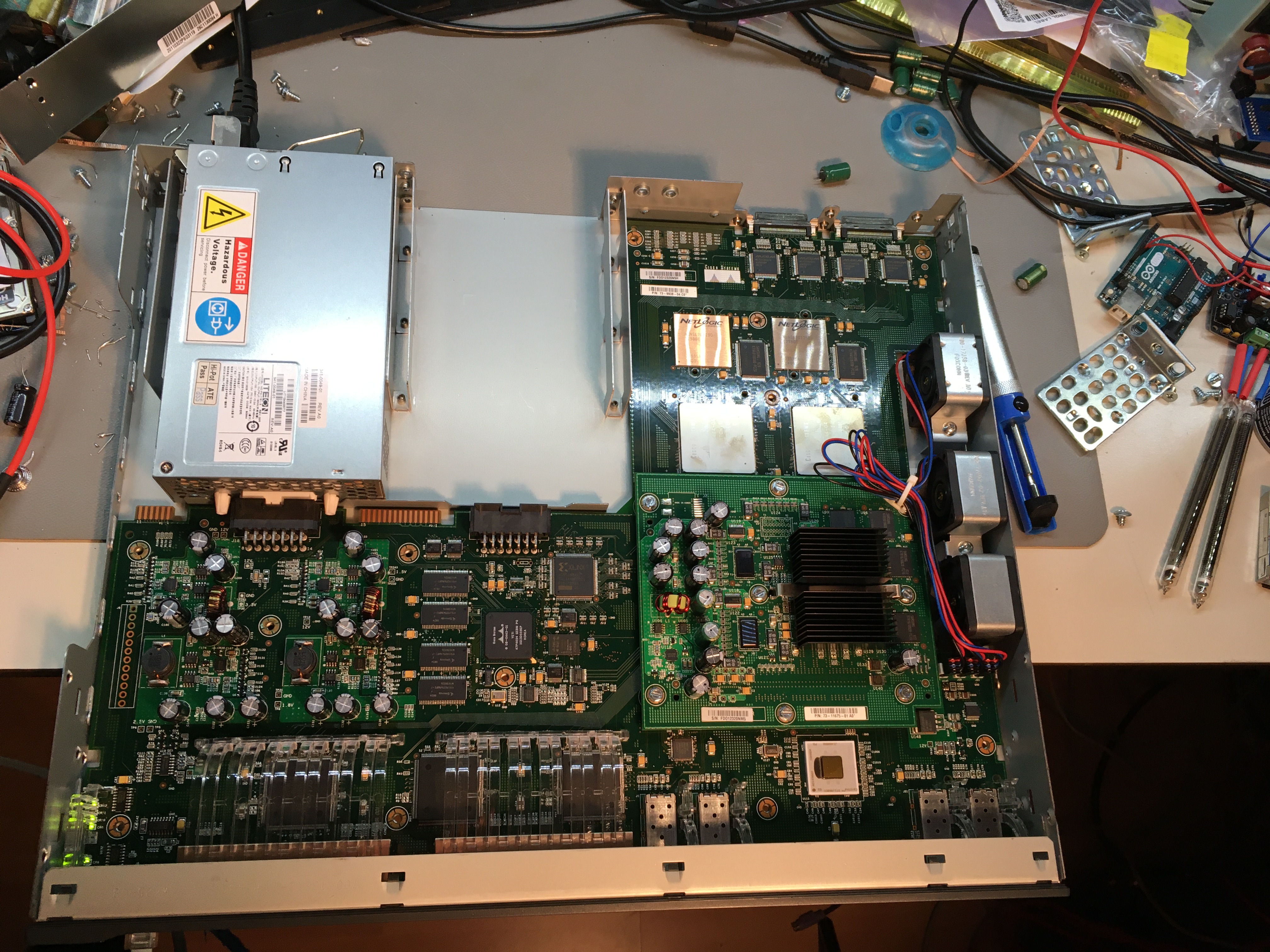
Before I can play around with this PB200, the device needs a  repair. I bought this device as a “none working, for parts”. And well.. it sure is in a “none working” condition, since the device doesn’t power on, at all.

That is one of the reasons I bought this device. When a device is not able to power on, this normally means the Power Supply (PSU) has a problem. The downside of this is of course that their is no easy way to test the rest of the functionality of the device.

Assessment of the problem

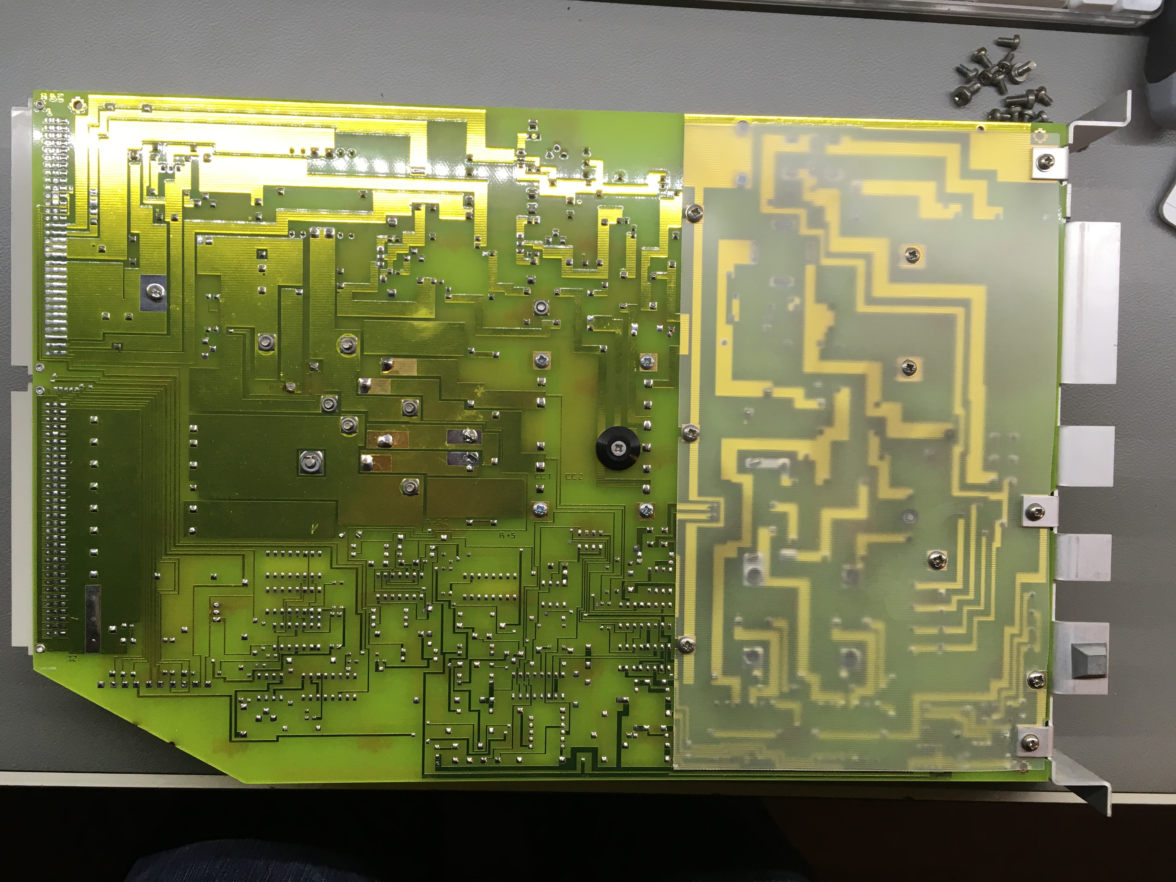
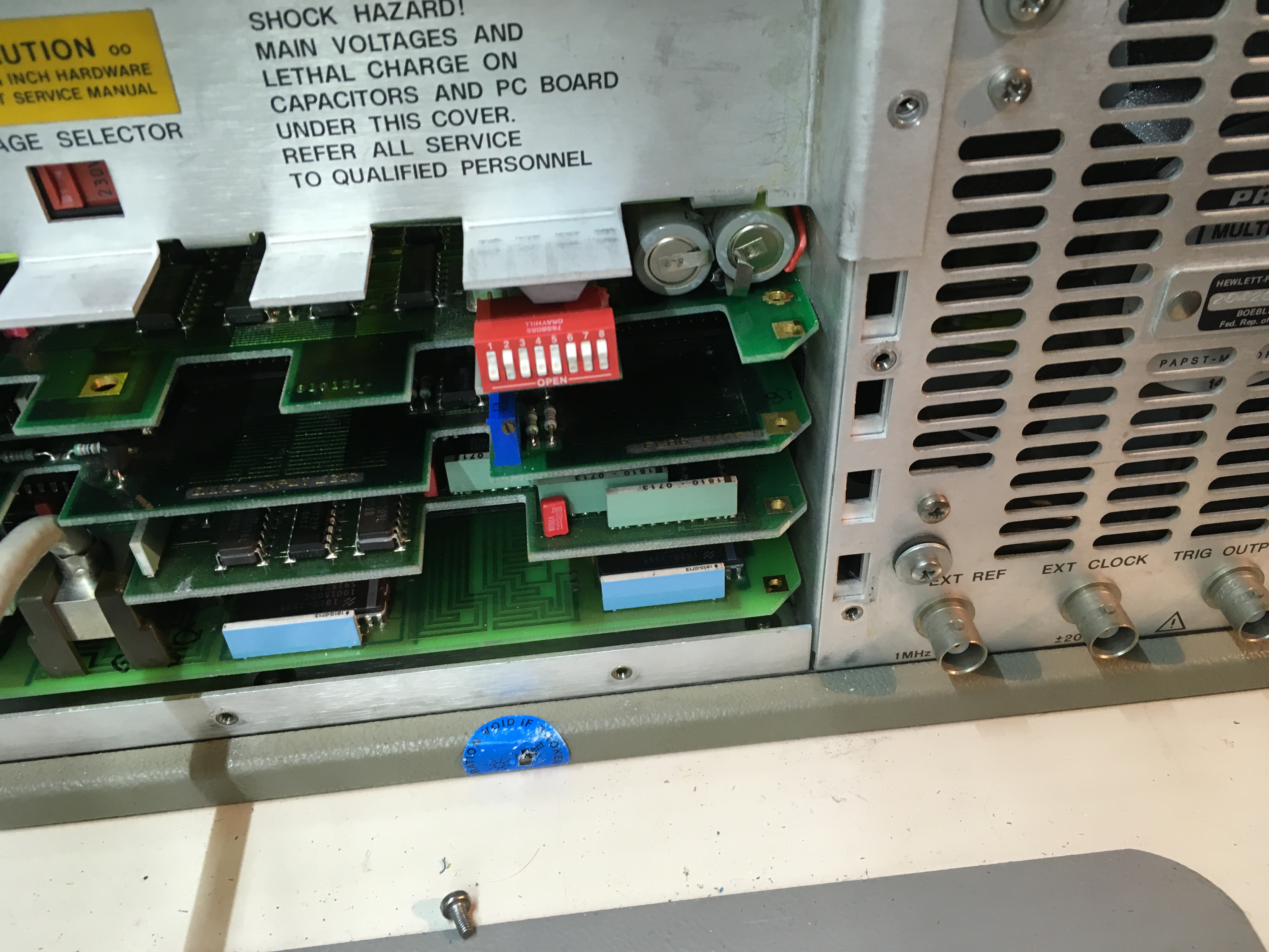
Once the devices arrived at my doorstep, I could inspect it further. And I noticed a sharp bent in the front panel once I removed the covers.  Not a good sign to start with. The second thing I ran into is that this device is a complete nightmare to take apart. The construction is just horrible. Screws on places which are heard to reach. I suspect this is just a branded by Tektronix. I got my hands on some Tektronix equipment, and repaired some, and the construction is always good engineered. In this case, it’s definitely not.

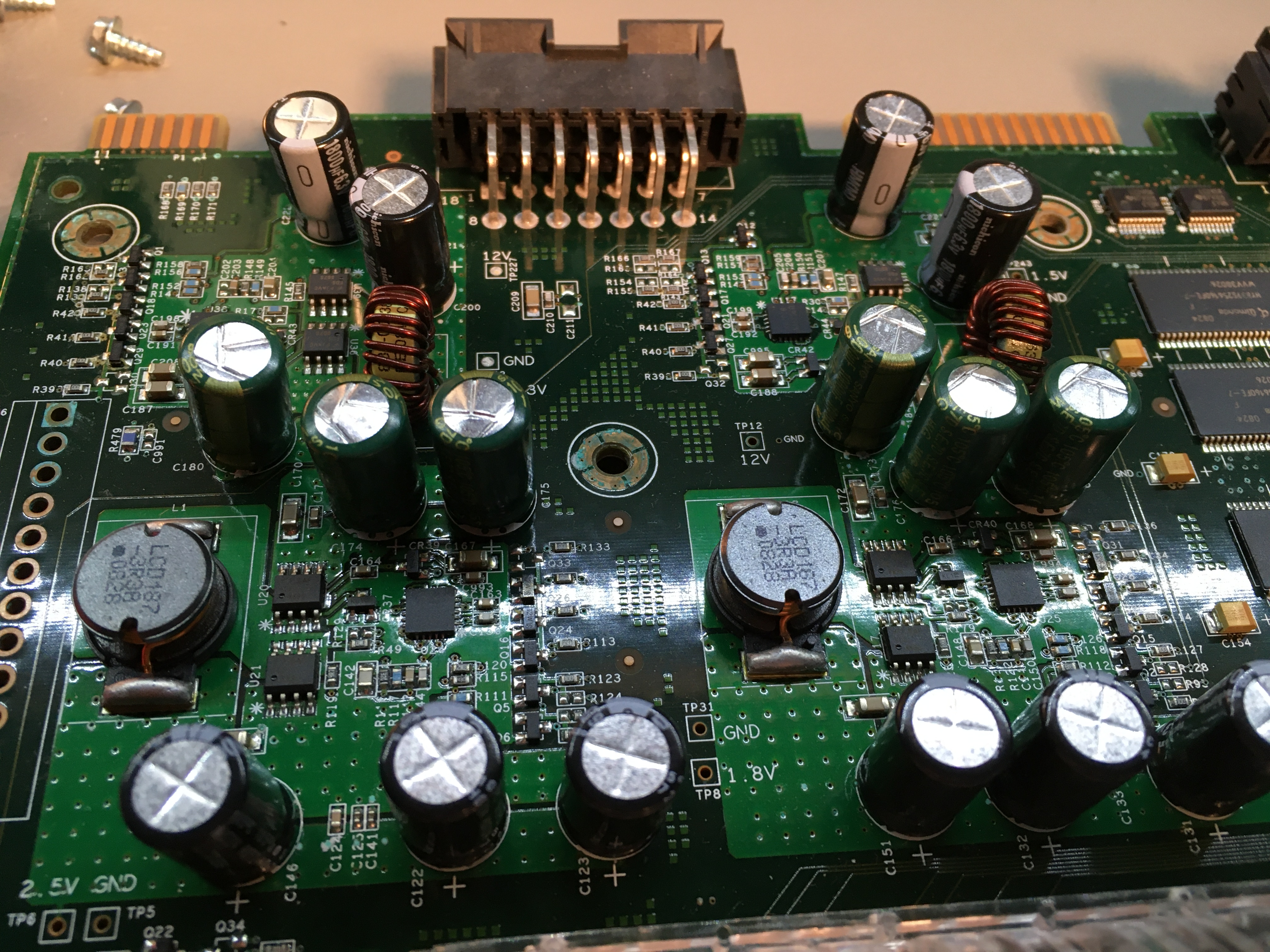
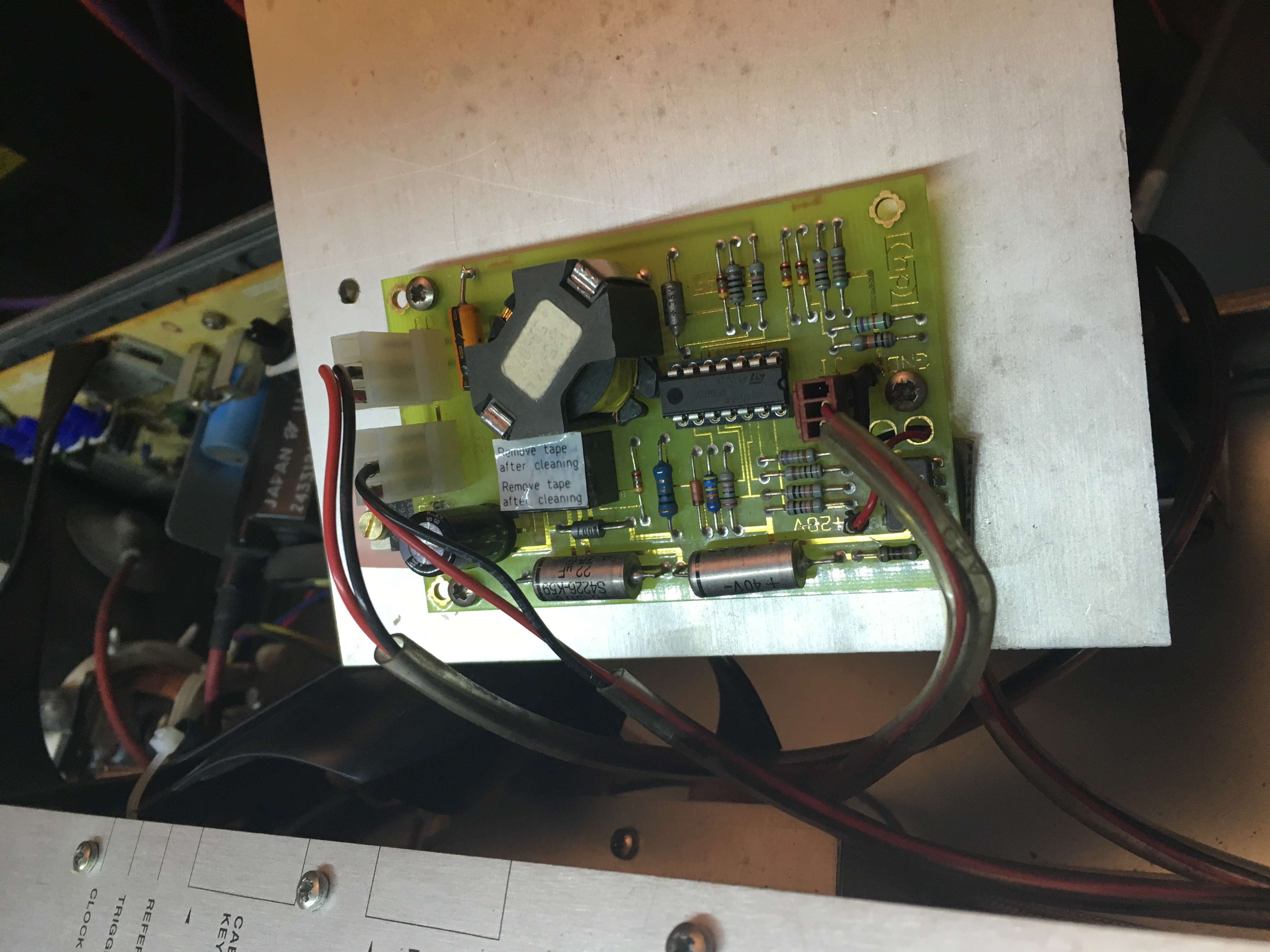
So it took a lot of effort to get the PSU out of the chassis. Once the PSU was out I noticed a burned up diode, and a burned spot on the PCB. A quick check of the fuse confirmed: This PSU had a very bad moment. This means that on the primary side of the PSU a lot of other components could be damaged. So the first thing I did was to hunt for a Service Manual, and well these cannot be found.

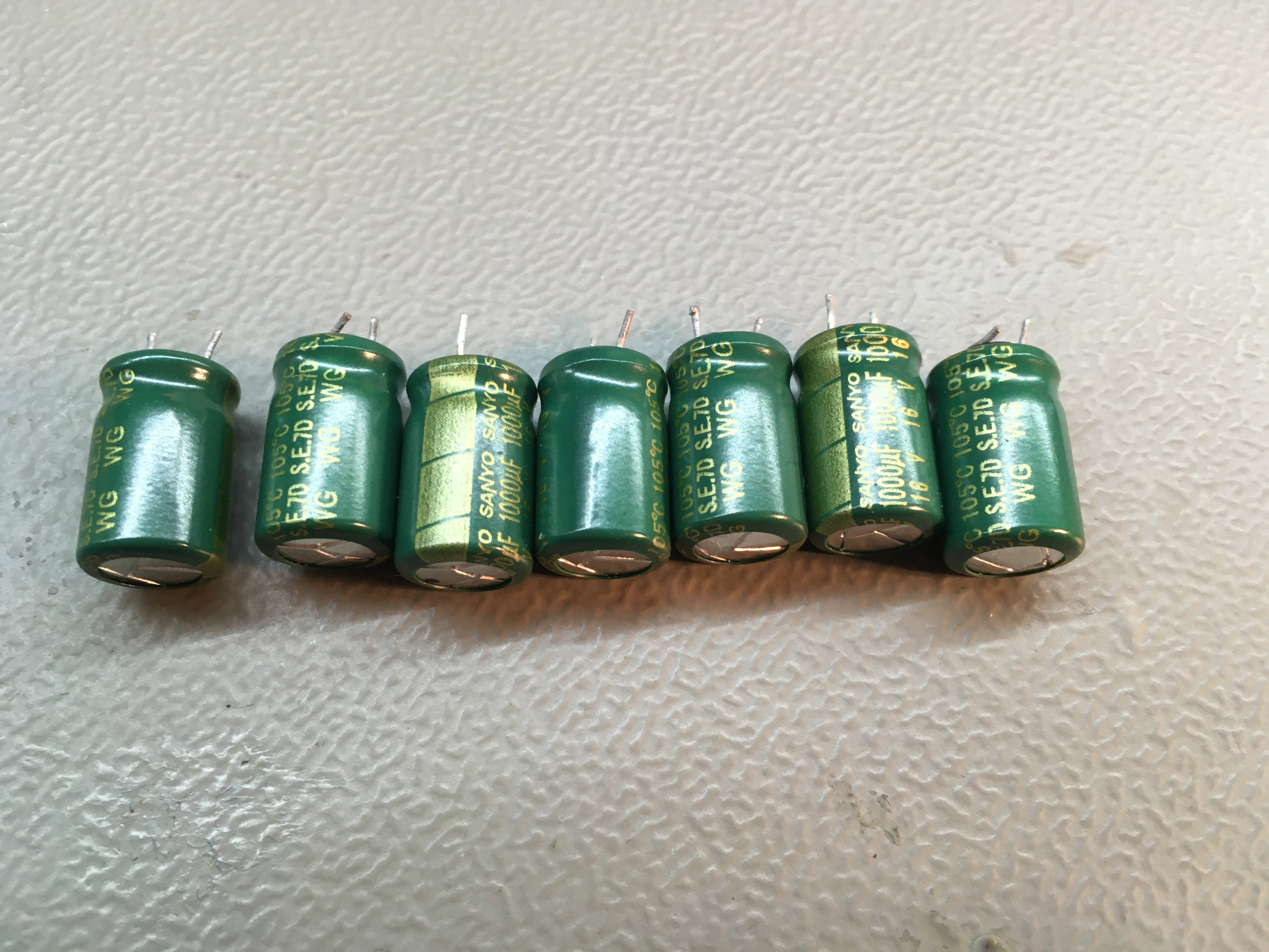
So I started to de-solder the diode, so I could get a marking of the component. The diode was next to some transistors, or MOSFETs so I decided to desolder them as well, since they are most likely also damaged , or are the cause of the damage.

While taking the diode out carefully, I could not prevent it from falling apart.


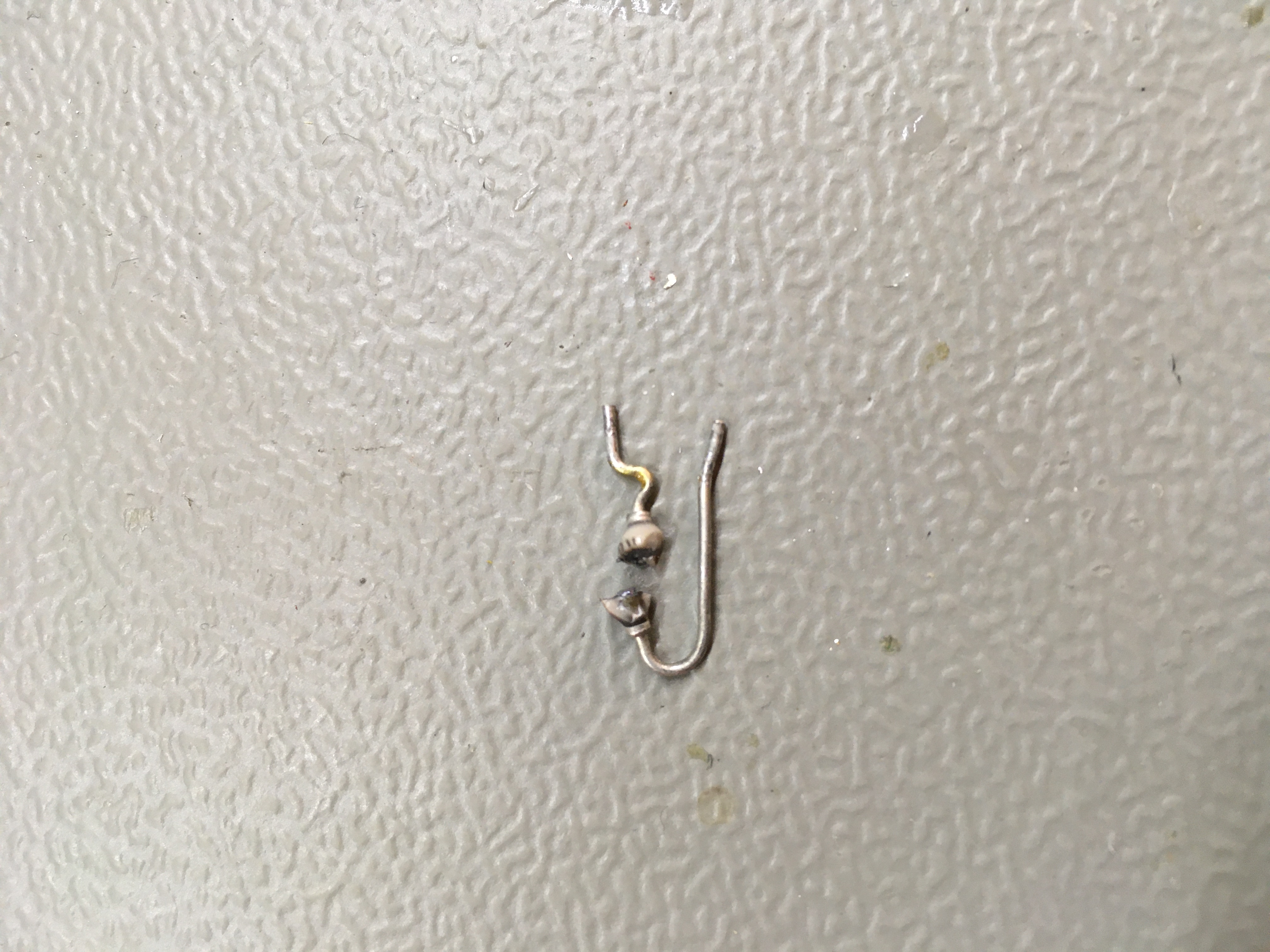
The diode literally exploded and split into halve. With a lot of trouble I managed to get some marking, but I wanted to make sure that I got it right. Primary side of a PSU always makes me nervous. So I started a [thread] on the EEVblog forum.

Another member also suggested to get a PSU replacement, which is almost the same. The only difference is the output voltage.

So I decided to buy this PSU, so I have a reference, and if I’m unable to repair the primary side of the PSU I could perhaps convert the secondary side so it gives the right voltages.

In part [two] I’m trying to fix the PSU

Repairing a Tektronix BP200 BERT tester – part two

An attempt to fix the primary side of the PSU

I started  to measure and test several components, and found some diodes which where shorted. Replaced them. However I could not measure any voltages after the full bridge rectifier. Some components are mounted on large heat-sinks. Removing them to get access to the components and be able to read the markings or to test them out of circuit, would be a pain.

Fighting with this power supply for a couple of evenings, I decided to take another route. In the meantime the alternative PSU was delivered. After comparing both the PSU’s together I noticed that only one voltage rails was different.

Modifying an PSU

Since fixing the primary side of the PSU would be very difficult to do, I started to look at the secondary side. Both the PSU’s are from the same series. So I figured the manufacturer probably used a couple of zener diodes, and resistors to control the output voltage. So I started to swap out diodes and resistors which where different and which I could relate to the voltage rail I wanted to adjust.

The moment of truth

I powered to PSU up, and measured all the good voltages (they where a little higher, but that’s okey since no load is attached.). I decided to go for it, and placed the PSU on top of the chassis, so I could test the PSU without going through the rather complex method of installing the PSU.

And after connecting the main power, and flipping the power switch, the PB200 came back to live.


A few quick tests showed me that the generator and analyzer are working without any problems. And I refitted the PSU back into the PB200.


Repairing Rohde & Schwarz SMT03 RF Signal Generator – part one

The R&S SMT03

The R&S SMT03 is a RF signal generator which can generate signals from 5Khz up to 3Ghz, while the signal level can be from -144dBm to +13dBm with 0.1dBm resolution.

A datasheet of the R&S SMT03 can be found [here]

Signal generators like the SMT03, and other (for example the HP ESG series like the E4421B) are mainly used to test communication devices and a like. Signal generators like this, are not arbitrary signal generators (however they may have an option to generate LF (Low Frequency) signals like square, sine, sawtooth wave-forms.

RF Signal generators generate sinus signal, and can generate different modulations (FM,PM,AM etc). These signal generators are a specialized piece of equipment.

An R&S SMT03 with problems

The SMT03 I’ve got in the LAB has some problems:

    • A few lines are visible on the LCD screen
    • When the unit is on for some tine, above 1.8Ghz the error: 110 Output Unleveled ALC failure is displayed .

The lines on the LCD screen are somewhat annoying, they don’t influence the working of the unit. The ALC Unleveled error does. When I try to measure the signal, the level is all over the place, and has a low level.  I noticed that in the short time this error is not present I can loose up to 4dBm when I generate signal above 1.8Ghz.

The challenges

When trying to fix an error like this, it’s important to understand the error. At the time this error presented itself, I didn’t had access to a Service Manual. And from the User manual I didn’t got any wiser. So after some thinking I concluded that ALC must stand for: Attenuation Level Control

This leads me to the conclusion that a possible cause could be a PLL circuit which is unable to establish a successful lock.  The bad news is: this may be due to a lot of other problems:

    • The input frequency may be of, or the signal is to low
    • Power problem (low / not working power rail
    • Mixer problem
    • And a lot of other related problems

Trying to diagnose the problem futher

So to diagnose such a problem, a block diagram and a schematic would be very helpful. But I got neither of them.

Another challenge is that the unit consists of modules, which plug into a back-plane. Operating the modules outside of the  unit seems only possible with a “service kit” which I don’t have access to, and cannot find any information about.

Despite the fact I don’t have the above items, I can observe the error, and take a look at how the physical signal path. So I opened the unit by removing the covers. Which is a simple and straightforward process: By unscrewing the bumpers on the back of the unit the top and bottom covers come off.

R&S SMT03 on the inside

Tracing from the output connector the signal path back I noticed that:

  • From the output connector, the signal is going through an attenuator, and then straight into a 3Ghz module (W154).
  • From the 3Ghz module the signal is entering an 1.5Ghz module (W104).
  • From this module the signal is going to a synth module, and a signal generator module.

And this tells me that the 3Ghz module has some kind of “pass-through”, so that signals up to 1.5Ghz are passed through the 3Ghz module (not sure at this point if some additional filtering is done). When signals are above 1.5Ghz the 3Ghz module generates the frequencies from 1.5 till 3Ghz.

This could mean that the ALC Unleveld error is somewhere in the 3Ghz module. Which means I could leave all the other modules alone.

For a moment I was thinking about a possible power rail problem, however this is most unlikely, since I aspect that for every frequency the ALC Unleveled error should be displayed, or that other errors would pop-up.

To summarize

    • Working on these units is not easy
    • A Service manual would be a great help

In [part 2] I’m going to try to repair this R&S SMT-03


Repairing Rohde & Schwarz SMT03 RF Signal Generator – part two

Trying to find a service manual

In part one I looked at the problems, and could conclude that the ALC error I’m seeing is most likely generated in the 3Ghz module.

So I started searching for the Service manual, and the ones I could find have description on the working of the modules, but the schematic and part lists these descriptions refer to, are not included. Without schematics this is already complicated, but without part numbers, most likely impossible.

Most of the components are SMD, and their markings are not always very descriptive. For example: A09 is this a A with the number zero, or the capital letter “O” ? or a component with just H2 on it won’t help either.

While I was searching for a service manual I investigated the error even more, since the error manifest itself when the unit gets warmer.

So I let the unit run for quite some time, and quickly removed the 3Ghz module, so I could feel where most of the heat is generated. Since these spots are the most likely candidates.

Taking a look inside the 3Ghz module

At that point I was at the end of the troubleshooting I could do. So I started to disassemble the 3Ghz module. Which got a lot of screws. And this is also the first time I opened a RF module. And at first glimpse, these kind of PCB look intimidating. Some RF parts and arrangement looks like RF black magic. But at the end of the day, it’s just a bunch of SMD components, and some specific RF stuff. Which I hopefully don’t have to mess around with. I also noticed a scratch on the PCB, where the scratch is coming from I don’t know, but it looks like someone worked on this module before.

the R&S SMT03 3Ghz module

While I was studying the layout of the 3Ghz module I made a list of possible components which could be the problem. The ALC error tells me that the problems must be before the signal leaves the module. Once the signal leaves the module, there is no way of detecting the level of the signal.

So may first plan of attack was to replace every opamp in the signal path, closest to the connector where the signal would leave the module.

Finally I found the Service Manual for the R&S SMT03

While making the list, a kept on searching to find the service manual. And to my surprise I found [here] the service manual with schematics, and most importantly a list with components.

Once I had the service manual I also could read the the 3Ghz uses the top cover as a heat shield. And from my experience I already notices how hot the module could get. So Without any proper cooling I don’t want to run this module without any covers. Which complicates troubleshooting even more.

But I figured: Since I’m already on the path of “guessing”  let’s continue with it. After studying the schematics, I picked a few places where the ALC error could come from.

Got it fixed

Long story short: I replaced all the opamps (which are 3 or 4) in the RF detection section, replaced 3 opamps in the 1.8Ghz filter range. And swap out some ceramic capacitors in the hot spots.

R&S SMT03 3GHZ sections where parts are replaced.

Of course, did didn’t solve the ALC error. After studying the schematics more, the only place could be the amplifier or pre-amplifier section.

While going ever the PCB I noticed someone replaced a component, since there was a lot of residue left. And this confirms that someone had worked on this module before. Was this also the person cause the scratch on the PCB ?

Could this be the cause of the 110 output ALC error ?

The component “A09” is on the other side of the module: This component turns out the be a “Hewlett Packard MSA-0986 Silicon Bipolar MMIC Amplifier”

This part is not easy to get, but I did mange to find it on Ebay. And as soon as it arrived, I replaced this part. And I could clean up most of all the residue.

The result after replacing the component and cleaning up the residue

As it And as it turns out, this part was the cause of the ALC error. I let the unit run for a couple of hours (fully assembled, so with all the covers on) and the error was gone.

The 110 ALC output error is gone

While this is not my preferred way of fixing It payed of in the end. Mainly because I could pin point the problem to a specific module, and I notices the work of someone else.

This brings me to another point: Lately I noticed on Ebay that prices has gone up for second hand , broken equipment. A R&S SMT03 with a lot of problems still cost over $500 or even $700 dollars. Fixing these units without a proper service kit is very hard to do. Especially if like me, lacking RF skills. For a trained electronics engineer, it’s more easy.  I think I just got luckily. But beware of units like this, and their (hidden) problems.


Repair of a Cisco 3750ME switch

A switch stopped working

Don’t you hate that ? Just starting a new lab, powering up the required hardware, and then to find out a crucial switch powered on just fine.. it worked for some time, and then stops working.

I for sure hate this, but in this case I thought: Well this looks like a power supply (PSU) failure. The switch in question is a Cisco 3750ME switch. And has swap-able PSU’s. So I swapped the PSU, but the switch won’t power on.

Time to take a closer look

Since I figured out it’s not a PSU failure I started to take the switch apart. After removing the cover, I measured the voltage line. There is a test point on the main board which makes it easy to measure the 12V power rail. And I measured no voltage what-so-ever.

So I unplugged the switch from the mains, and measured a short between the ground and the +12v. Which didn’t surprise me at all. After opening the switch, I noticed a few capacitors which bulged.

Repair time

So I started to take the switch completely to bits, since the main board has to come out.  Their are a lot of screws. And taking the main board out is not that easy.  But once the main board came out, I could start de-solder the capacitors which were bad. And this was a time consuming job. The mainboard is a multilayer board, with large copper plains, and getting the capacitors out was a real hassle.

All the capacitors which had gone bad, were of the same type and values:

16V 1000uF

Taking them out was a real pain in the b*tt, soldering the new ones in, was not easy. After spending a couple of hours I manged the solder every cap back in.

A few tips on (de)soldering components on multi-layer PCB

Soldering or de-soldering parts on a multi-layer PCB can be tricky, and difficult to do. First of all: take your time. Be patient, and don’t try to damage the PCB. So don’t use sharp screwdrivers on the PCB while trying to pry components of the board. If you damage a track or tracks, it can be hard or impossible to repair.

Use a soldering iron with enough watts. Multi-layer PCB’s can have large ground planes. And these ground plains can take a lot of heat. If you don’t have a soldering iron with enough power, you can (if you have one) use a hot air gun to preheat the board. Don’t set your hot air gun to hot. You don’t want to de-solder any other tiny components.

In this case, the capacitors where through hole components. And with these components one tricks works very well: Heat up one leg of the component. Wiggle or pull the component from the board with your fingers. Make sure you don’t burn yourself in the process. Let this leg cool down, and start heating the other leg. Apply pressure to the component again, lifting it from the board. Then let this leg cool down, and start heating the other leg again.  And by heating each leg, gong back and forth and gentle forcing the component from the PCB.

Once the component is removed, the holes can still hold a small portion of tin, making it impossible to insert a new component. Getting the tin out of the holes can be a tedious process as well. First thing to try is to use a lot of flux, and fresh tin. Just fill the holes with fresh tin, and try to suck the tin out with a de-solder pump.  You can also to try to use solder wick.

Don’t try to heat up the hole to long. You may damage the hole itself, or the PCB tracks around it. And that can be the end of the game. If you can’t get the tin out, the next may work as well:

Get a small needle and a pliers. Grap the needle with the pliers, and place the sharp point of the needle into the hole. Heat the hole and the needle with the soldering iron, and gentle (don’t apply to much pressure) puss the needle through the hole. Once all the tin is melted, wiggle the needle around, and pull it back up again. This way you may get enough tin out, the place the new component.

Finally result

Once I soldered all the capacitors back in I started to reassemble the switch. Putting the main board back into the chassis, was not easy. After some tries I figured out it’s best to remove the light pipes, insert the main board, and place the light pipes on the main board once the main board is in place.

And as soon the board was completely assembled, I connected the switch to the mains, and it powered up with out a problem. Next I ran some diagnostics on the switch and it looked fine again. Last step was to place the cover back on again, and placing the switch back into the rack.

How to connect GNS3 virtual appliance to OSX Mojave

How to connect GNS3 virtual appliance to OSX Mojave

When working with GNS3 lab, it’s easy to connect the virtual lab to the internet. This is simply done by using the “cloud” and connect it to a wired interface (wifi adapter won’t work).

The problem with this setup is that the virtual GNS3 lab is not accessible from the local system. In my case a Macbook Pro. And since I almost use wifi connection, I don’t have a physical interface to bind to. When using virtual appliances which in turn have web GUI’s, it can be very annoying when those devices can’t be reached from a browser on the local system.

Searching for a solution, I came across a solution to install a tuntap package, but this package won’t work on Mojave.

Luckily there is an other and easy solution when using GNS3 with vmware Fusion. Once GNS3 and vmware Fusion is installed, and started, Fusion creates so called “vmnet” interfaces. This may also be the case when using VirtualBox, but I haven’t tested it.

So keep in mind that this solution has a short coming, being that there is no connection to the Internet. Depending on the local network setup, it should be possible to go through the trouble of setting op routes. But in my case I don’t need Internet access from the virtual lab.

These interfaces have an ip address (let’s say 192.168.4.1) When placing the “cloud” in GNS3, just add a vmnet interface:

Make sure to tick the box “Show special Ethernet interfaces”

Select the vmnet interface from the pulldown menu and click on the “Add” button. The vmnet interface should now appear in the box below, where the interface can be selected.


Next connect the vmnet interface to the cloud, and connect the virtual appliance to the cloud. Give the virtual appliance an ip adres in the same subnet (192.168.4.x/24) The virtual lab should now be reachable from the local system.

Playing around with a IV-3A VFD tube

What is a VFD tube ?

VFD IV3-A display

I got my hands on four IV-3A VFD tubes. When I started to learn about these tubes, I called them “Nixie tubes”, but that is wrong, very wrong. The more I learned about VFD tubes, the less I called them “Nixie tubes”.

So what is a VFD tube ? Well, VFD stands for: “Vacuum Fluorescent Display” And that is the first big difference with a Nixie tube. A Nixie tube is NOT a vacuum tube, a Nixie tube is filled with a gas (neon gas).

A lot of information on how a VFD tube works, can be found online (and Nixie tubes as well of course).  According to Wikipedia:

A VFD operates on the principle of cathodoluminescence, roughly similar to a cathode ray tube, but operating at much lower voltages. Each tube in a VFD has a phosphor coated anode that is bombarded by electrons emitted from the cathode filament.[1] In fact, each tube in a VFD is a triode vacuum tube because it also has a mesh control grid

For more info see: Vacuum fluorescent display

A VFD tube is not a Nixie tube

The difference between a Nixie and a VFD tube. On the left a Nixie tube, on the right a IV3-A VFD tube
On the left A Nixie tube and on the right a VFD tube

Often I see a VFD display are sold/advertised as being a “Nixie tube” However a VFD display is not a Nixie tube. Compared to a Nixie tube, the Nixie tube has “stacked numbers” (cathodes). And a wire-mesh of anodes.  And each number lights up when a high voltage is applied  to one of the cathodes.


A Nixie tube works with voltages above 100 Volts (around 180 Volts).  A VFD tubes needs multiple voltages for the heater, grid and the segments. The heater voltages are usually around 1V, and the grid and segments are in the range of 20 – 30 Volts.

So a VFD works with much lower voltages then a Nixie tube.

Another difference between  a VFD and a Nixie tube is that a VFD is a vacuum tube, whereas a Nixie tube is filled with a neon gass.

Getting the IV-3A tube to work

It took a lot of searching to find information about the IV-3A tube. Since these tubes where produced in Russia, the datasheets for the tubes are also in Russian. And I don’t speak, and cannot read Russian.  I did found some info, for instance on the EEVBLOG Forum, where I found the voltages and Amperes needed for the heater. But I could not find information about the pin-out of the IV-3A tube. What I could find, is that the pin-out is the same as the IV-6 VFD tube.

A good friend of mine, Dave gave me an excellent tip: to use the Google translate app, and scan the PDF with my phone’s camera. This worked to some extend. The translation was not perfect, but gave me the last pieces of information I needed to get the IV-3A tube working.

The technical specs of the IV-3A tube

The IV-3A tubes needs the following voltages:

  • Heating voltage: 0,7 … 1 V
  • Grid voltage: 20 … 30 V
  • Anode-segments voltage: 20 … 30 V
  • Current of heating: 25 … 35 mA
  • Grid current: no more than 12 mA
  • Current of the anodes-segments: no more than 0.45 mA
  • Readiness time: not more than 0.2 s;

The pinout of the IV3A is simple: There is a wire cut off. This wire also has no internal connections. This wire is the “index wire” This is pin 12.  Pins 7 and 8 are the heather (cathode). One of these pins must be connected to gnd, and the other pin must be connected to a positive voltage (0.7 .. 1V).

Pin 9 is the grid pin, this pin must be connected to 20 .. 30V. The rest of the pins are the different segments (so pins 1,2,3,4,5,6,10,11) When these pins are connected to 20..30V a segment lights up. When a segment pin is connected to GND, the segment is “off”.

So to connect the IV3-A tube, and to test if all segments work, connect pin 7 to gnd, and pin 8 to +0.7V. Next connect pins 1,2,3,4,5,6,10,11 and pin 9 to +20V (don’t apply the max voltage of 30V to long, this will shorten the life of the tube). If the tube is working you should see all the segments lit.

See the datasheet of the IV-3A here (this PDF is part of Dieter’s Nixie- and display tubes data archive datasheet of the IV-3A


How-to read and write a HEX file from Arduino/ATMEGA328P

When things go wrong with an Arduino sketch

Maybe you recognize this one: When working on hobby projects, and most likely multiple ones, it can take a long time for a project reaches its final stage. And well some projects don’t seem to end at all.

One of the projects I’m working on is a frequency counter. And this is just one of those projects where I work on for a couple of weeks, and then it ends up collecting dust. And after a long period of time I start working on it again.

The downside is that after a long periode of time (in this case  a couple of years) you can’t remember everything what is done during the project. Especially when it comes down to software. I’m not a full-time developer so setting up a git hub repository is not a “natural thing”.

And that caused an interesting situation: I finally came around to develop PCB’s for the frequency counter. And of course the first version of the PCB had some faults in it. So I started to fix those faults, and made a second version of the PCB main board.

Once I soldered the second version I uploaded the sketch to the ATMEGA-328P which I’m using to drive the display and some other things.

After days of troubleshooting I finally figured out it was the software which caused problems. The sketches I had didn’t work. So I only got a ATMEGA-328P which I took from the bread-board, and that ATMEGA-328P is working fine.

I didn’t want to reverse engineer the complex sketch, so I figured: If I can take the binary code from the original ATMEGA-328P and then upload the binary file to a new ATMEGA-328P I can at least go further with test the hardware.


Getting the HEX file from a existing ATMEGA-328

Since I use a Imac (running Mojave) the command to read the hex file from an ATMEGA-328p:

/Applications/Arduino.app/Contents/Java/hardware/tools/avr/bin/avrdude -C ./Java/hardware/tools/avr/etc/avrdude.conf -v -v -v -v -pm328p -c arduino -P/dev/cu.usbmodem14401 -D -Uflash:r:/~/freq_cnt.hex:i

To write the hex file:

/Applications/Arduino.app/Contents/Java/hardware/tools/avr/bin/avrdude -C/Applications/Arduino.app/Contents/Java/hardware/tools/avr/etc/avrdude.conf -v -patmega328p -carduino -P/dev/cu.usbmodem14401 -b115200 -D -Uflash:w:/~/freq_cnt.hex:i

When using the commands above, make sure to change the USB device ( the part after the “-P” flag. And also the place to save or read the HEX file from.

How to setup an Electronics lab

So how do you setup a electronics lab?

I did read a lot of articles, forums, and watched a fair amount of YouTube movies about how to set up a electronics lab. However in all those articles, and movies I missed a few things, which in my opinion,are essential even before you set up a lab in the first place. And so I think a better question is: What kind of electronics lab to setup ?

Before getting to setup a lab

Once you get involved into electronics, there comes a point you need equipment, to do your electronics stuff. And if your going to read up on this subject, you will discover that in most cases, people will tell you get quite an amount of stuff. For example:

    • Get multi meter
    • Get even one more multi meter
    • Get a soldering iron
    • Get a decent scope (analog or digital, or both)
    • Get a lab power supply (PSU)
    • Get all kinds of pliers
    • Get screwdrivers an such
    • Get a function generator
    • Get a frequency counter
    • Get a shitload of components

You get the point. The list is endless, and it will cost you at least a 1000 euro’s to get a basic lab like this together.

So let’s stop here. And think about it for a moment. Once you get involved or want to get involved into electronics, there is a learning curve. In other words: What kind of electronics are you interested in ?

And when talking about electronics, I’m not talking about putting some Arduino modules together, and writing code. To me, that’s not electronics. That’s programming electronics. Once you get to the point in troubleshooting the modules itself, I call it electronics.

So when starting electronics, one of the basic things to get are: stuff to learn. Now you can go to any (online) bookstore, and buy a few kilograms of book’s about the subject, and starting out your own personal library. But you also can get a book, a few parts, and start building the projects which are described in the book.  A good example of this is the series: Make Electronics. The best part is: There are kits you can buy, which contains all the components.

Another approach may be to get an Arduino, or Raspberry PI, and some resistors, and LED’s and play around with these, and create small projects.
You may also need  one or two (small) breadboards.

In the example of the Make Electronics, the beauty of it is: you get a small stock of components, which you can play around with. Of course you need some tools, and the bare minimum is a multi-meter, and a soldering iron, and some cutting tools, to clip off some wires. One or two small pliers is a must.

However at this point, you’re not sure if your going to stick to this hobby, or that it’s fun, but not for you. If you start with the list a few lines back, you invested a lot into something you never going to use again. Of course you can sell it on, but there will be a loss of money.

Another important thing to think about is: get a dedicated place where you can practice or build your stuff. I reasonable workspace, to work at, is a must. This is most likely the place where you start building your electronics lab.

And once you learned some stuff, you may find a certain part of electronics interesting. That can be repairing like  audio, or analog stuff (old radio’s, receivers)  Maybe you like RF or HF stuff,  Or you really like to design stuff. Or you want to dive into digital stuff. In other words: Electronics is a broad area.

I started with a make electronics book, and once I played around with the 7400 series logic IC’s I was hooked, and wanted to learn more about digital stuff. Logically (pun intended) I started to put together a electronics lab, which is suited for troubleshooting digital stuff.

Once you get into a certain field of electronics, and you’re more sure that you keep involved into electronics, you may start to look around for equipment. Once at that point, getting a decent lab power supply, a scope and a function generator is a good way to go.

And once you know and understand these devices, and getting better in electronics in general, more specific equipment can be bought. If your into RF stuff, a Spectrum  Analyzer, when dealing with different protocols, and buses like I2C for example you may want to have a USB protocol / logic analyzer or a logic analyzer build into your oscilloscope. And sooner or later, you’re going to discover that buying equipment which is sold as “for parts or repair” is much cheaper, and that it can be fun to repair equipment. And doing so, you learn at the same time 🙂 However when you going to walk the path of ” I can like to fix stuff” The more likely it is that you’re getting more and more equipment, and a pile of electronic components.  And eventually run out of available space..

At the point you know what your interest is, it’s much easier to get a stock of components. You also know which equipment you need to get. This way setting up a electronics lab, you can keep the initial costs down. So to summarize:

To get a minimal electronics lab together, start with the basic stuff:

    • Learn Electronics, buy book, and a small kit of components
    • Multi meter
    • Create your own dedicated workspace
    • One or two breadboards
    • A couple of screwdrivers
    • One or two pliers

Once your convinced that electronics is something you really like to do, go out and buy a soldering iron. When building small projects on breadboards, you don’t need a soldering iron. However if you want to make the circuits permanent, you do need a soldering iron.

And when buying a multi meter, don’t buy a meter which is in below or in the 15 euro range. Just don’t. For 50 euro’s you can get a decent meter. Even if you don’t know if electronics is something for you, don’t buy the cheapest multi meter you can get. Because you really going to regret it.

Getting equipment like Multi-meters,Soldering iron, Scope etc.  is a topic on it’s own.


Refurbish a HP8175A

Refurbish a HP8175A

Both of the HP8175A’s have some issues. And that is to be expected when getting equipment which is from the 80’s.The first HP8175A I bought has the following issues which needs to be addressed:

    • Replace the blown filter RIFA cap
    • I noticed some heat-sinks on the processor board are loose
    • The capacitors on the Power Supply board must be replaced
    • General clean-up of the front panel and casing.The second HP8175A has the following issues:
    • The keyboard panel is loose
    • The capacitors on the Power Supply board needs replacing

On both of the machines I have to:

    • Replace the blown filter RIFA cap
    • Replace a leaking Nicad battety
    • General clean-up of the front panel and casing

So to get these devices in a good running condition takes some effort. But without a Service Manual, this can be complex tasks. I searched online for the service manual for days but could not find any. Looking on Ebay the manual is also hard to find, and when a listing for a Service manual pops-up, the prices are in my opinion way to high.

Replacing the capacitors

The power board. This board is really heavy. It’s a beautiful design board, with golden traces on back.

To be honest, replacing the capacitors can be done without a service manual. This however requires some thinking ahead. The silk screen on the board doesn’t list the polarity of the caps. So a good practise is to take detail photographs of the Power board. Some of the caps are hidden under heat-sinks, so it’s difficult to take a good picture.

What I ended up doing is to replace the caps one by one. So de-soldering one cap, put it aside, making sure I write down the polarity, and place the capacitor besides the PCB in the same orientation it came from the board.

Also before ordering the capacitors, make sure to get the right sizes, so they actually fit on the board. Here is the list of the capacitors I replaced (per device):

    • 4x 270uF 40VDC  lead spacing 5mm
      5x 470Uf 25VDC   lead spacing 5mm
    • 1x 330Uf 35V          lead spacing 5mm
    • 2x 1000Uf 200VDC  lead spacing 10mm (snap-in)
    • 2x 5600Uf 6.3VDC   lead spacing 10mm (snap-in) Note: these capacitors aren’t replaced.

I also soldered in the replacement for the RIFa cap: which is a 250V 0.022uF Y2 cap.

When replacing capacitors, or working on Power supplies: Know what you are doing. If you don’t feel comfortable working on PSU’s which can have high voltages in them, then don’t mess around with them. Always make sure to discharge any capacitor. Some capacitors may hold a lethal charge!


Testing after the capacitors are replaced

Once all the capacitors are changed, time to test if everything works. Before replacing the power board I double check the polarity of the capacitors. And I  Also recheck the voltages and capacitance. Just to make sure every capacitors is replaced by the correct one.

And Again things go boom!

Once every thing is checked I applied the power.. and a loud hissing noise, a bang.. and another capacitor exploded. After a quick inspection I find out that a capacitor on a board for the FANS had exploded. Luckily this is a 270uF 40VFC cap, which I got in stock, so I replaced the capacitor.

Next I had to figure out why the capacitor has blown. As it turns out I misaligned the connector for the fans, causing a short. After I placed  the connector correctly  I powered the HP8175A on again. The devices works! However I noticed the fans are now spinning at a high speed. Telling me there is some damage on the fan PCB.

And that is bad news. HP (but others like Tektronix ) like to use their own part numbers. So it’s really hard to tell which IC or component your dealing with. Having a Service Manual, with a part number reference table, and / or the schematic of the board would be very helpful. Unfortunately for this device the manual is hard to get.. or is it ?

Getting the Service Manual

Looking around the Keysight website I noticed I could send a support request. And so I did. I aksed for the Service Manual, and a few hours later I got a reply e-mail, with the requested service manual attached. So after all it was quite easy to get the service manual, and of course a big thank you to Keysight!

Getting the fans working again

The chip in the middle is the LM324 I had to replace

The service manual has no reference to a fan PCB board. Which doesn’t surprise me. The other HP 8175A doesn’t have this board installed, and the power board is a slightly different. Both of the fans are directly connected to this power board. But I was able to get the part numbers and as I suspected one of the IC’s is an opamp a LM324. And after replacing the opamp the fans working again, that is: they run at a much lower speed, being temperature controlled again.

Re-seating the heat-sinks

A lot of heat-sink came loose, so I had to glue them with a thermal compound back on to the IC’s.

The first time I took the first HP8175A apart after a filter cap had blown, I noticed a small black metal piece fall out of the machine. At that time I didn’t had a clue where this little heat-sink was coming from. I didn’t had take all the board out yet. But once I did, I find that the processor board was missing two heat-sinks. I started to feel if the other heat-sinks where still glued, and just touching the heat-sink made them come loose from the IC’s.

So I used some thermal compound to glue them back on again, and since one was missing I ordered a heatsink for a DIP-16 package online, and put that one in place as well.

Replacing the NiCad batteries

The leaky battery, this is nasty stuff.

The HP8175 have a 2.4V Nicad rechargeable battery which holds the configuration. This battery doesn’t hold any calibration, so it’s easy to replace them. However finding a exact replacement is not possible. (There is some New Old Stock (NOS), but since these batteries are very old, I don’t recommend buying and using them.


The new batteries installed, and it fits perfectly. The batteries are in series, and hot-glued together.

So I ended up buying four 1.2V batteries, and put two batteries together in series. (so I created 2 sets of 2 batteries)  I cleaned up the board carefully making sure to remove any acid from the leaked batteries. This stuff will eventually eat it’s way through the PCB, causing a lot of damage. The best way to clean this is with vinegar.  After that I cleaned the board with alcohol.

Cleaning up the front and case of the machines

I used some rubbing alcohol and other soft chemicals to clean up the front and the cases, and after that the machines looked a lot better. I also used some double-sided tape to stick the keyboard cover back on. And at this points both of the HP8175A are ready to be used again.

All in all it took some fair amount of time to get these machine usable again, but it was worth the effort. Especially taking into account  that these machines are fun to use and to play around with 🙂