Introduction
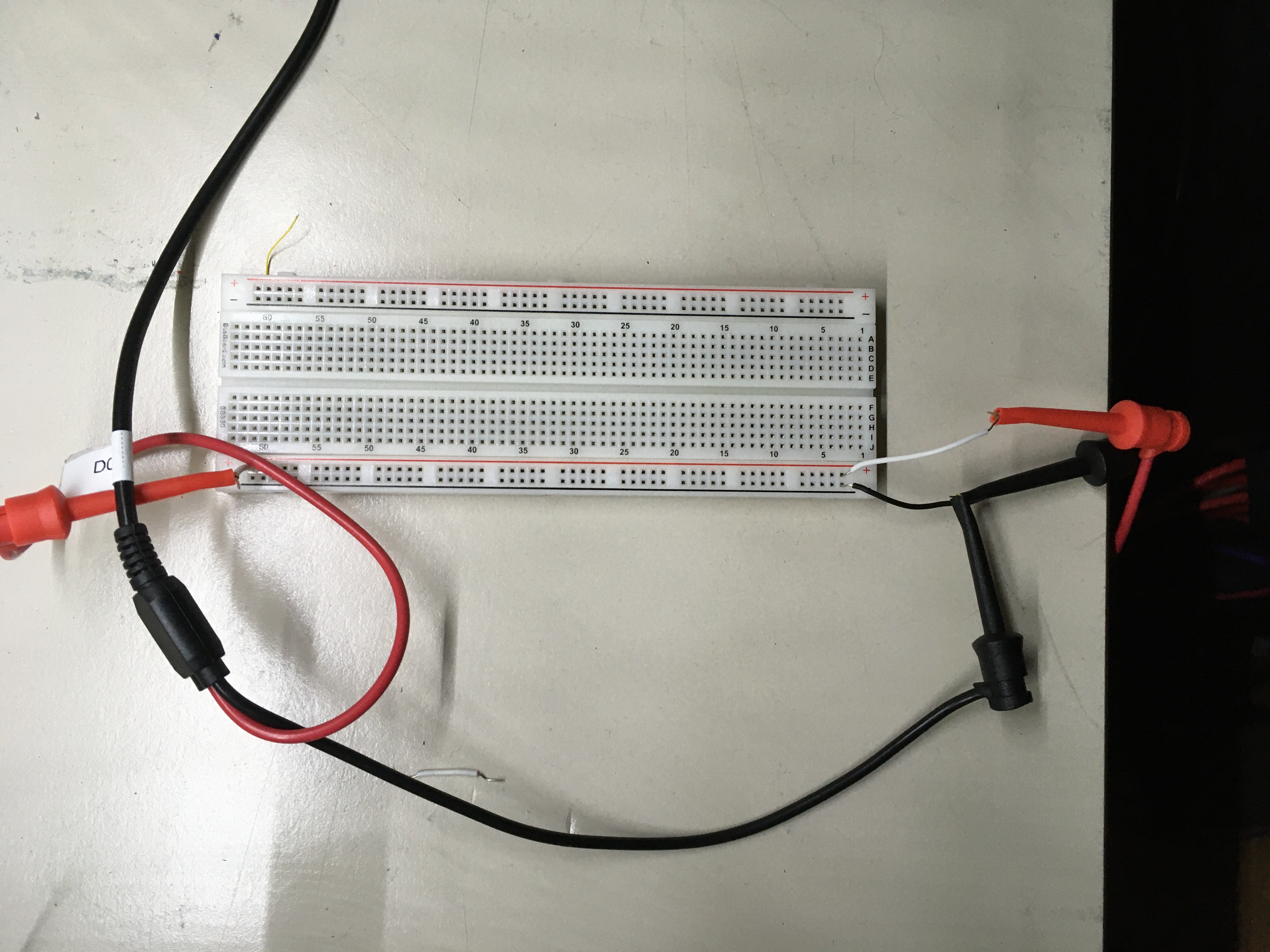
In part three the rest of the counter is build, and the circuit is almost complete. The part which is missing, is the thing that makes it count. We could simply add a 4 bits binary counter, but why not simulate a counter ?
The HP8175A
To simulate a simple 4 bits counter, I’m going to use my HP8175A. It’s big, it’s heavy, makes a lot of noise and eats a gazillion electrons per microseconds, and spits them out as heat. So what is not to love about this machine?
The interface of the HP8175A may take some time to get used at, but I loved it from the start. However to make it more interesting the HP8175A is programmed completely by IEEE-488. or GP-IB or a HP-IB If you own a HP8175A and don’t have the possibility to remote control the machine, then study the user manual. It’s really not that difficult to program the HP8175A through the keyboard and knobs.
I used a National Instrument USB GPIB HS adapter to remote control the HP.
Remote control the HP8175A
To program the HP8175A a couple of steps must be taken. The HP8175A has so called “Module pages”. We need to:
-
- Setup on the Data Module the format: by setting up the POD and the duration.
- Setup on the Data Page the labels and bits which makes up the program
- Setup on the Program Page the program, the start end end labels, as well the times to run the program
- Setup the Clock page,
- And finally update all the settings and start the program
The IEEE-488 commands for the HP8175A is a bit cryptic, but this is the whole program:
RST
DM0;DUR0,1s;IFM(CLOCK),,,1111
DM1;CFM(CLOCK);TSA0;CHD0,(CLOCK),0000,0001,0010,0011,0100,0101,0110,0111,1000,1001;TSA9;CHD0,(END)
PM0;CD;(PROG1);CR7;CE;(END)
OM;POD 1
CM 0;CYM 1
UP;SA
LO
Explanation of the program
The commands and parameters are separated by a ‘;’. So for example the second line contains 3 commands: DM0 and DUR0 and IFM (Data Module, Duration Fixed, and Insert ForMat label)
-
- Reset HP8175A to defaults
- Go to page: Data Module FORMAT and set DUration to fixed 1 second and Insert ForMat label CLOCK and enable the first 4 POD lines (bits) of POD0
- Go to DATA page module and ChangeForMat label to CLOCK and Set
- ToStartAdress; CHangeData 0, CLOCK end set bits up to address 9 and change label to END ()
- Go to Program Module page and set the label PROG1, Move Cursor Right 7 positions, clear the field and change field so it contains the END label
- Go to Output Module page and set all PODS enable
- Goto Clock Module page and Set Clock to Auto Cycle
- Update and start
- Return to local (stop remote control, and enable front panel)
Line 3 might require some explanation:
DM1;CFM(CLOCK);TSA0;CHD0,(CLOCK),0000,0001,0010,0011,0100,0101,0110,0111,1000,1001;TSA9;CHD0,(END)
The part:
TSA0;CHD0,(CLOCK),0000,0001,0010,0011,0100,0101,0110,0111,1000,1001
is quite clever. The engineers at the time by HP really know how to implement this kind of stuff. The command TSA needs a start address, which is the 0. Next command changes the format label to “CLOCK”. And then comes the clever part.
Since we enabled only for outputs on POD 0, we can have 4 bits on each address line. So by placing the 4 bits separated by comma’s, each bit pattern is placed on a address line. And therefore, this command places each 4 bits starting from address 0000 to 1001 (0 – 9).
So it works like:
                 4bits  4bits                                4bits
Set start addr   addr 0 addr 1                               addr 9
/|\               /|\   /|\                                   /|\
 |                 |     |                                     |
TSA0;CHD0,(CLOCK),0000,0001,0010,0011,0100,0101,0110,0111,1000,1001

DECIMAL              0,   1,   2,   3,   4,   5,   6,   7,   8,   9
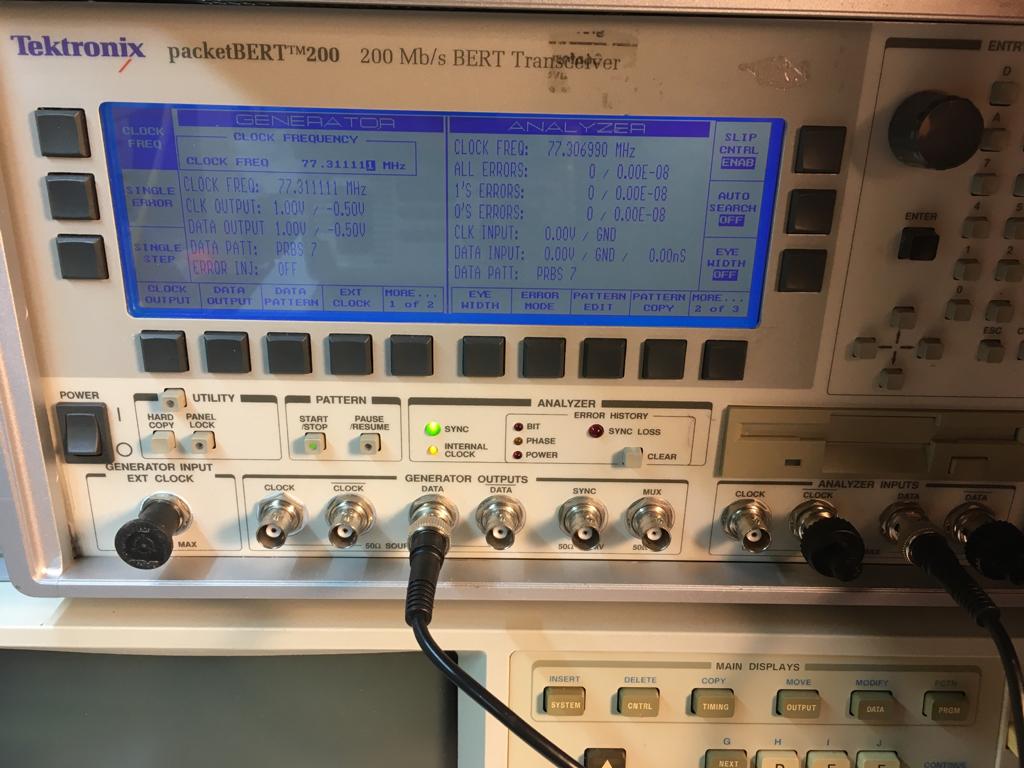
Let’s see the HP8175A in action
After sending the commands, the HP8175A is acting like a 4 bit binary counter:
Once I know the program is working I wrote a little pyton script using pyvisa:
import pyvisa
import time

# Small programm to remote control a HP8175A
# Using PyVisa with a NI USB GPIB-HS+

# Setup the resource manager
rm = pyvisa.ResourceManager()

#print(rm.list_resources())
# Open HP8175A
hp8175a = rm.open_resource('GPIB0::8::INSTR')

# Identify yourself!
print(hp8175a.query('IDN?'))
print(hp8175a.write('RST'))
time.sleep(5)

print(hp8175a.write('RST'))
print(hp8175a.write('DM0;DUR0,1s;IFM(CLOCK),,,1111'))
print(hp8175a.write('DM1;CFM(CLOCK);TSA0;CHD0,(CLOCK),0000,0001,0010,0011,0100,0101,0110,0111,1000,1001;TSA9;CHD0,(END)'))
print(hp8175a.write('PM0;CD;(PROG1);CR7;CE;(END)'))
print(hp8175a.write('OM;POD 1'))
print(hp8175a.write('CM 0;CYM 1'))
print(hp8175a.write('UP;SA'))
print(hp8175a.write('LO'))